
How to design an active rectifier - schematic
In this tutorial, we are going to design an active rectifier in CMOS 180 nm, including the design of the schematic and layout considerations.
Schematic Design
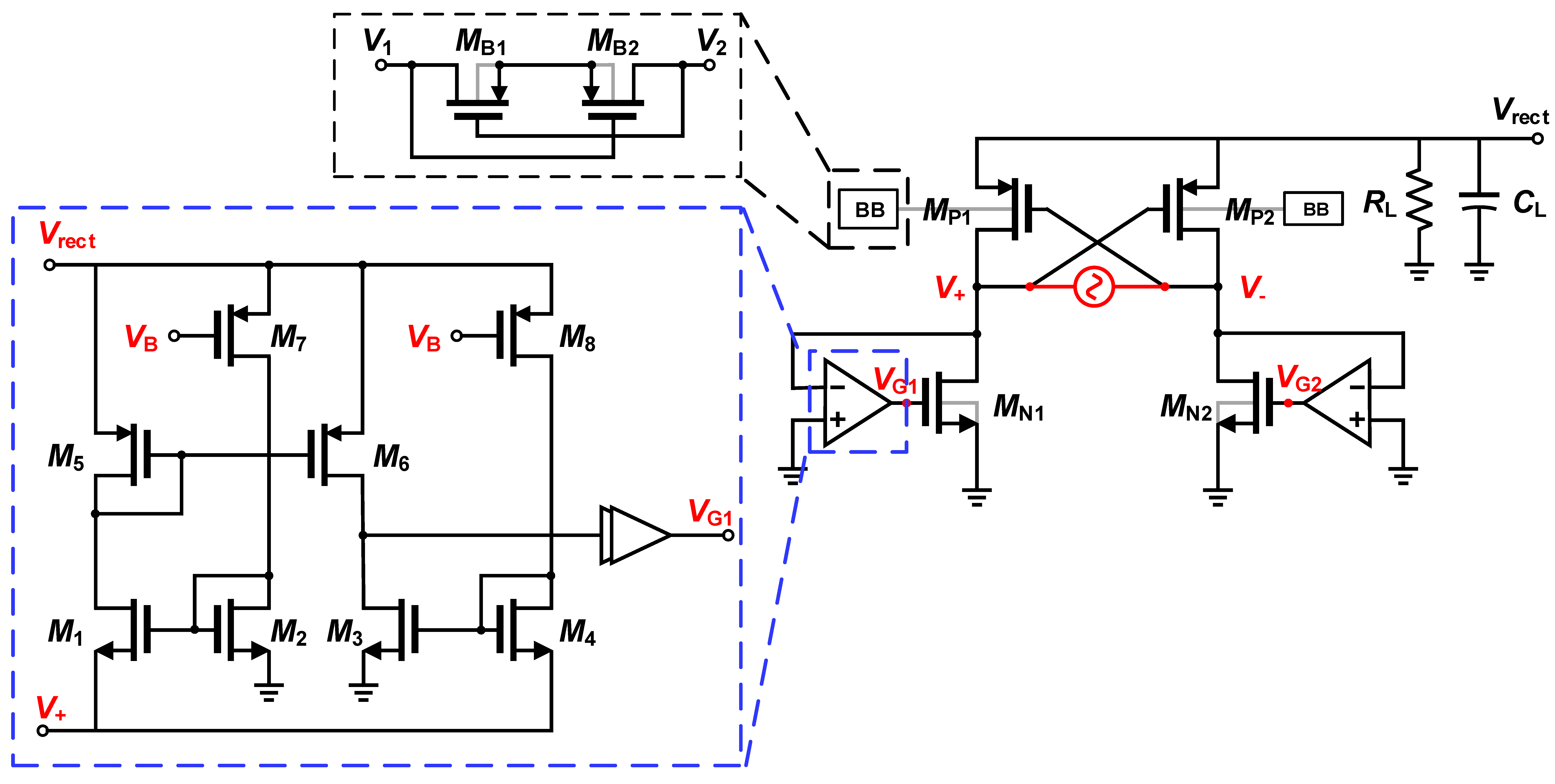
This rectifier consists of three main components, as shown in Fig. 1:
- Cross-coupled PMOS transistors: These transistors serve as switches to transform the sine wave input into a steady voltage output by charging the load capacitor (CL).
- Active diodes with common-gate comparators and buffers: Using comparators, these active diodes detect the point where the input voltage crosses zero. This information is then used to control the on/off state of the NMOS transistors.
- Self bulk bias (BB): To ensure the PMOS transistors are optimally biased, a self bulk bias mechanism is employed. This helps determine the highest voltage from the input and rectified voltage.
By employing cross-coupled PMOS transistors as switches, the rectifier stabilizes the input sine wave, charging the load capacitor (CL) for a constant voltage output. The active diodes, aided by comparators and buffers, detect zero crossings in the input voltage, enabling control over the NMOS transistor switching. This design outperforms diode-connected NMOS setups, yielding a higher voltage conversion ratio (VCR). To ensure proper biasing for the PMOS transistors, the self bulk bias (BB) mechanism identifies the peak voltage from both input and rectified sources.
Common-Gate Comparator
The two comparators CMP1 and CMP2 are common-gate push-pulldifferential-input comparators, with the bias currents provided by M7and M8. As described above, when VAC2– VAC1> |Vthp|, MP2 is turned on, and V+ keeps going down.When VAC1 swings below 0 V, M1 of CMP1 sinks a largercurrent than M2 does. As M4 is diode-connected,therefore, VG4 drops with V+, and reduces VGS3. Thecurrent of M1 is mirrored to M6 through M5, causingM6 to source a larger current than M3 can sink, thusdriving Vrect as well as VGN1 high and turns on theactive-diode switch MN1. In the other half cycle, V+ goes up and V-goes down, then MN2 will be turned on in a similar manner andconducts current from ground to Vrect through the AC source.
Take IM7=I1 and IM8=I2,IM5=I3, IM6=I4,1 and IM3=I4,2,VG4=V1 and VG2=V2. I1, I2are assumed constant, so V2 and VGS4 will be constant.
Simulation Results
In this section, we delve into the simulation outcomes and the impact of various parameters on both power conversion efficiency (PCE) and voltage conversion ratio (VCR). For instance, Figure 2 provides insight into the rectifier's behavior through a transient simulation spanning 5 microseconds. As depicted, it requires close to 1 microsecond to attain a stable state. Additionally, the graph reveals the gate voltage trends of the active diodes. Notably, these diodes activate precisely when the input voltage (Vin) intersects the zero-crossing point.

Moreover, Figure 3 displays the current usage during switching, covering both NMOS and PMOS transistors, along with comparator consumption. The main reason for power loss, leading to lower power conversion efficiency (PCE), is the delay in activating the switching active diodes. This delay results in reverse current leakage within the rectifier. To tackle this, a potential solution is to improve the comparator's design. This enhancement can effectively address the issue, leading to better overall performance of the rectifier.

Transistor Sizing Effect on PCE and VCR
In this part, we will explore how adjusting the size of the power MOSFETs (3.3V IO CMOS) impacts the voltage conversion ratio (VCR) and power conversion efficiency (PCE). Figure 4 illustrates the influence of NMOS (MN1,2) width on PCE and VCR, while Figure 5 demonstrates a similar impact for PMOS (MP1.2) width. On the other hand, when aiming to conserve space, it's advisable to opt for the smallest feasible transistor sizes. For example, for NMOS and PMOS widths, values like 0.6 mm and 16 mm could be considered suitable choices.

